

Why semiconductor additive manufacturing is challenging—and what comes next

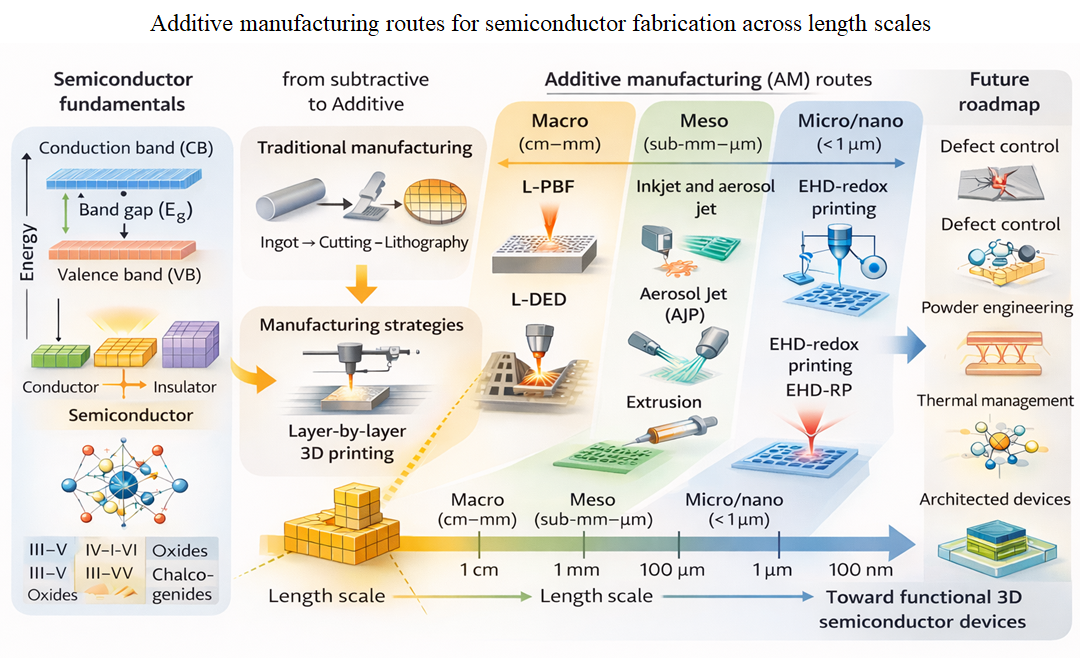
Semiconductors underpin modern electronics, optoelectronics, sensing, and energy technologies, yet their manufacturing remains dominated by centralized, tool-intensive, and largely planar process flows. Additive manufacturing (AM) offers a complementary pathway that can reduce material waste, accelerate prototyping, and unlock three-dimensional (3D) semiconductor architectures that are difficult to realize using conventional fabrication. However, AM of semiconductors is still in its infancy and has been demonstrated for only a limited set of materials and processes. This perspective synthesizes the current landscape of semiconductor AM by compiling reported 3D-printable semiconductor systems and mapping them to the corresponding AM techniques, including laser powder bed fusion, selective laser sintering, gas-phase reactive AM, inkjet printing, electrohydrodynamic redox printing, two-photon lithography, aerosol jet printing, extrusion-based AM, and laser-directed energy deposition. The key process-specific barriers are critically discussed—spanning feedstock limitations, densification and cracking, stoichiometry control and volatilization, texture and compositional heterogeneity, post-processing burdens, contamination, and scalability. On this basis, a length-scale–guided roadmap is proposed: laser powder bed fusion is positioned as the most promising route for cm–mm thermoelectric architectures, with advances in substrate/feedstock design, atmosphere control, and microstructure/defect engineering; ink-based and reactive approaches are highlighted for sub-mm to micro-scale functional devices through improved ink chemistry, 3D buildup, and multi-material integration; and electrohydrodynamic redox printing/two-photon lithography are identified as leading candidates for sub-micron to nanoscale fabrication, where material diversification, low-temperature conversion, residue mitigation, and hybrid integration with conventional microfabrication are essential. Collectively, this perspective clarifies terminology, consolidates the emerging evidence base, and outlines research priorities required to transition semiconductor AM from proof-of-concept demonstrations toward robust, application-relevant device manufacturing.
- Sze SM, Li Y, Ng KK. Physics of semiconductor devices. 4th ed. Hoboken, NJ, USA: John Wiley & Sons; 2021.
- Streetman BG, Banerjee S. Solid state electronic devices. 7th ed. New Jersey, USA: Prentice Hall; 2016. Available from: https://rrsdce.wordpress.com/wp-content/uploads/2018/07/sspd-eee-swapnil.pdf [Last accessed on 2026 Feb 06].
- Askeland DR, Phule PP, Wright WJ, Bhattacharya D. The science and engineering of materials. 2003. Available from: https://anupturnedworld.wordpress.com/wp-content/uploads/2016/06/askeland-the-science-and-engineeringof-materials.pdf [Last accessed on 2026 Feb 06].
- Perez N. Physical Properties of Solids. In: Perez N, editor. Materials Science: Theory and Engineering. Berlin/Heidelberg, Germany: Springer Nature; 2024:739-788. doi: 10.1007/978-3-031-57152-7_14
- Chen C-Y, Retamal JRD, Wu I-W, et al. Probing surface band bending of surface-engineered metal oxide nanowires. Acs Nano. 2012;6(11):9366-9372.doi: 10.1021/nn205097e
- Yin Y, Yang Y. Sustainable Transition of the Global Semiconductor Industry: Challenges, Strategies, and Future Directions. Sustainability. 2025;17(7):3160. doi: 10.3390/su17073160
- Peter Y, Cardona M. Fundamentals of semiconductors: physics and materials properties. Berlin/Heidelberg, Germany: Springer Science & Business Media; 2010. doi: 10.1007/978-3-642-00710-1
- Pierret RF. Semiconductor device fundamentals. Boston, MA, USA: Addison-Wesley Publishing Company; 1996. Available from: https://s3-us-west-2.amazonaws.com/valpont/uploads/20151124213927/Semiconductor_Device_Fundamentals1.pdf [Last accessed on 2026 Feb 06].
- Granqvist CG. Handbook of inorganic electrochromic materials. Amsterdam, The Netherlands: Elsevier; 1995. doi: 10.1016/B978-044489930-9/50001-5
- Wang QH, Kalantar-Zadeh K, Kis A, Coleman JN, Strano MS. Electronics and optoelectronics of two-dimensional transition metal dichalcogenides. Nat Nanotechnol. 2012;7(11):699-712. doi: 10.1038/nnano.2012.193
- Snyder GJ, Toberer ES. Complex thermoelectric materials. Nature Mater. 2008;7(2):105-114. doi: 10.1038/nmat2090
- Poelking CR. The (Non-) Local Density of States of Electronic Excitations in Organic Semiconductors. Berlin/Heidelberg, Germany: Springer; 2017. doi: 10.1007/978-3-319-69599-0_7
- Gratzel M. The light and shade of perovskite solar cells. Nature Mater. 2014;13(9):838-842. doi: 10.1038/nmat4065
- Baliga BJ. Fundamentals of power semiconductor devices. Springer; 2018. Available from: https://link.springer.com/book/10.1007/978-3-319-93988-9 [Last accessed on 2026 Feb 06].
- Hasan MZ, Kane CL. Colloquium: topological insulators. Rev Mod Phys. 2010;82(4):3045-3067. doi: 10.1103/RevModPhys.82.3045
- Geim AK, Grigorieva IV. Van der Waals heterostructures. Nature. 2013;499(7459):419-425. doi: 10.1038/nature12385
- Sze S. VLSI technology overviews and trends. Jpn J Appl Phys. 1983;22(S1):3. doi: 10.7567/JJAPS.22S1.3
- Vaidya AA, Adithya R, Aravind Raj S. Additive Manufacturing for the Semiconductor Industry: An Automotive Perspective. In: Metal Additive Manufacturing: Methods, Materials and Applications. Berlin/Heidelberg, Germany: Springer; 2025:387-402. doi: 10.1007/978-981-96-8162-4_21
- Craton MT, Konstantinou X, Albrecht JD, Chahal P, Papapolymerou J. Additive manufacturing of a W-band system-on-package. IEEE Trans Microw Theory Tech. 2021;69(9):4191-4198. doi: 10.1109/TMTT.2021.3076066
- Hu C, Jahan S, Yuan B, Panat R. 3D‐AJP: Fabrication of Advanced Micro-architected Multi-material Ceramic Structures via Binder‐Free and Auxiliary‐Free Aerosol Jet 3D Nanoprinting. Adv Sci. 2025;12(15):2405334. doi: 10.1002/advs.202405334
- Lu LL, Lu YY, Xiao ZJ, et al. Wood‐inspired high-performance ultrathick bulk battery electrodes. Adv Mater. 2018;30(20):1706745. doi: 10.1002/adma.201706745
- Lai W, Erdonmez CK, Marinis TF, et al. Ultrahigh-energy‐ density micro-batteries enabled by new electrode architecture and micropackaging design. Adv Mater. 2010;22(20):E139-E144. doi: 10.1002/adma.200903650
- Yee DW, Lifson ML, Edwards BW, Greer JR. Additive manufacturing of 3D‐architected multifunctional metal oxides. Adv Mater. 2019;31(33):1901345. doi: 10.1002/adma.201901345
- Shi J, Chen X, Wang W, Chen H. A new rapid synthesis of thermoelectric Sb2Te3 ingots using selective laser melting 3D printing. Mater Sci Semicond Process. 2021;123:105551. doi: 10.1016/j.mssp.2020.105551
- Gayner C, Kar KK. Recent advances in thermoelectric materials. Prog Mater Sci. 2016;83:330-382. doi: 10.1016/j.pmatsci.2016.07.002
- Narvan M, Ghasemi A, Fereiduni E, Kendrish S, Elbestawi M. Part deflection and residual stresses in laser powder bed fusion of H13 tool steel. Mater Des. 2021;204:109659. doi: 10.1016/j.matdes.2021.109659
- Balbaa M, Ghasemi A, Fereiduni E, Al-Rubaie K, Elbestawi M. Improvement of fatigue performance of laser powder bed fusion fabricated IN625 and IN718 superalloys via shot peening. J Mater Process Technol. 2022;304:117571. doi: 10.1016/j.jmatprotec.2022.117571
- Fereiduni E, Ghasemi A, Elbestawi M. Selective laser melting of aluminum and titanium matrix composites: recent progress and potential applications in the aerospace industry. Aerospace. 2020;7(6):77. doi: 10.3390/aerospace7060077
- Yu K, Yao Y, Zhang W, et al. Defects, monitoring, and AI-enabled control in soft material additive manufacturing: a review. Virtual Phys Prototyp. 2025;20(1):e2588456. doi: 10.1080/17452759.2025.2588456
- Wang YM, Voisin T, McKeown JT, et al. Additively manufactured hierarchical stainless steels with high strength and ductility. Nat Mater. 2018;17(1):63-71. doi: 10.1038/nmat5021
- DebRoy T, Wei HL, Zuback JS, et al. Additive manufacturing of metallic components–process, structure and properties. Prog Mater Sci. 2018;92:112-224. doi: 10.1016/j.pmatsci.2017.10.001
- Yu K, Zhang W, Lu L, et al. MG-LDM: A multimodal guided latent diffusion model with Mamba-based temporal encoding for inverse topological design of tissue engineering skin substitutes. Adv Eng Inform. 2026;71:104275. doi: 10.1016/j.aei.2025.104275
- Han C, Fang Q, Shi Y, Tor SB, Chua CK, Zhou K. Recent advances on high‐entropy alloys for 3D printing. Adv Mater. 2020;32(26):1903855. doi: 10.1002/adma.201903855
- ISO. ISO/ASTM 52900:2021(en) Additive manufacturing-general principles-fundamental and vocabulary. Available from: https://www.iso.org/obp/ui/#iso:std:isoastm:52900:ed-2:v1:en [Last accessed on 2026 Feb 06].
- Cao C, Xia X, Shen X, et al. Ultra-high precision nano additive manufacturing of metal oxide semiconductors via multi-photon lithography. Nat Commun. 2024;15(1):9216. doi: 10.1038/s41467-024-52929-8
- Zhang H, Hobbis D, Nolas GS, LeBlanc S. Laser additive manufacturing of powdered bismuth telluride. J Mater Res. 2018;33(23):4031-4039. doi: 10.1557/jmr.2018.390
- Welch R, Hobbis D, Birnbaum AJ, Nolas G, LeBlanc S. Nano‐and micro‐structures formed during laser processing of selenium doped bismuth telluride. Adv Mater Interfaces. 2021;8(15):2100185. doi: 10.1002/admi.202100185
- Qiu J, Yan Y, Luo T, et al. 3D Printing of highly textured bulk thermoelectric materials: mechanically robust BiSbTe alloys with superior performance. Energy Environ Sci. 2019;12(10):3106-3117. doi: 10.1039/C9EE02044F
- Zhan R, Lyu J, Yang D, et al. Large-scale SHS based 3D printing of high-performance n-type BiTeSe: Comprehensive development from materials to modules. Mater Today Phys. 2022;24:100670. doi: 10.1016/j.mtphys.2022.100670
- Mao Y, Yan Y, Wu K, et al. Non-equilibrium synthesis and characterization of n-type Bi 2 Te 2.7 Se 0.3 thermoelectric material prepared by rapid laser melting and solidification. Rsc Adv. 2017;7(35):21439-21445. doi: 10.1039/C7RA02677C
- Baudry M, Savelli G, Roux G. 3D printing of bulk thermoelectric materials: Laser powder bed fusion of N-type silicon germanium. Mater Sci Eng B. 2023;298:116897. doi: 10.1016/j.mseb.2023.116897
- Welch R, Gubisch S, Leblanc S. Nano/microstructures and thermoelectric properties of silicon germanium manufactured using laser powder bed fusion. J Mater Process Technol. 2025;337:118749. doi: 10.1016/j.jmatprotec.2025.118749
- Wu K, Yan Y, Zhang J, et al. Preparation of n‐type Bi2Te3 thermoelectric materials by non‐contact dispenser printing combined with selective laser melting. Phys Status Solidi (RRL)–Rapid Res Lett. 2017;11(6):1700067. doi: 10.1002/pssr.201700067
- Lai Z, Guo T, Zhang S, et al. Selective laser melting of commercially pure silicon. J Wuhan Univ Technol-Mater Sci Ed. 2022;37(6):1155-1165. doi: 10.1007/s11595-022-2647-3
- Shi J, Chen H, Jia S, Wang W. 3D printing fabrication of porous bismuth antimony telluride and study of the thermoelectric properties. J Manuf Process. 2019;37:370-375. doi: 10.1016/j.jmapro.2018.11.001
- Gagnon JC, Presley M, Le NQ, Montalbano TJ, Storck S. A pathway to compound semiconductor additive manufacturing. MRS Commun. 2019;9(3):1001-1007. doi: 10.1557/mrc.2019.114
- Berkson MA, Pogue EA, Bartlett ME, et al. Evaluation and Mitigation of Impurities in Additively Manufactured Epitaxial Gallium Nitride. Cryst Growth Des. 2024;24(8):3149-3159. doi: 10.1021/acs.cgd.3c01163
- Tran V-T, Wei Y, Yang H, Zhan Z, Du H. All-inkjet-printed flexible ZnO micro photodetector for a wearable UV monitoring device. Nanotechnology. 2017;28(9):095204. doi: 10.1088/1361-6528/aa57ae
- Tran V-T, Wei Y, Du H. Influence of thermal treatment on electronic properties of inkjet-printed zinc oxide semiconductor. Int J Smart Nano Mater. 2022;13(2):330-345. doi: 10.1080/19475411.2022.2084172
- Nydegger M, Pruška A, Galinski H, Zenobi R, Reiser A, Spolenak R. Additive manufacturing of Zn with submicron resolution and its conversion into Zn/ZnO core–shell structures. Nanoscale. 2022;14(46):17418-17427. doi: 10.1039/D2NR04549D
- Oh H, Charles H, Im T, Khan H, Lee CS. Extrusion-based additive manufacturing of three-dimensional MoSe2-nanosheet-coated TiO2 hetero-structures for photocatalytic CO2 reduction. Int J Adv Manuf Technol. 2024;130(5):2731-2742. doi: 10.1007/s00170-023-12869-x
- Lee J, Choo S, Ju H, et al. Thermoelectric Generators: Doping‐Induced Viscoelasticity in PbTe Thermoelectric Inks for 3D Printing of Power‐Generating Tubes (Adv. Energy Mater. 20/2021). Adv Energy Mater. 2021;11(20). doi: 10.1002/aenm.202170076
- Le Dantec M, Abdulstaar M, Leistner M, Leparoux M, Hoffmann P. Additive manufacturing of semiconductor silicon on silicon using direct laser melting. Berlin/Heidelberg, Germany: Springer; 2017:104-116. doi: 10.1007/978-3-319-66866-6_10
- Yue W, Zhang Y, Zheng Z, Lai Y. Hybrid laser additive manufacturing of metals: a review. Coatings. 2024;14(3):315. doi: 10.3390/coatings14030315
- Vargas-Bernal R, He P, Zhang S. Hybrid Nanomaterials: Flexible Electronics Materials. BoD–Books on Demand; 2020. doi: 10.5772/intechopen.83326
- Menetrey M, Koch L, Sologubenko A, Gerstl S, Spolenak R, Reiser A. Targeted additive micro-modulation of grain size in nanocrystalline copper nanostructures by electrohydrodynamic redox 3D printing. Small. 2022;18(51):2205302. doi: 10.1002/smll.202270276
- Gramlich G, Huber R, Haslich F, Bhutani A, Lemmer U, Zwick T. Process considerations for Aerosol-Jet printing of ultra fine features. Flex Print Electron. 2023;8(3):035002. doi: 10.1088/2058-8585/ace3d8
- Ghasemi A, Fereiduni E, Balbaa M, Elbestawi M, Habibi S. Unraveling the low thermal conductivity of the LPBF fabricated pure Al, AlSi12, and AlSi10Mg alloys through substrate preheating. Addit Manuf. 2022;59:103148. doi: 10.1016/j.addma.2022.103148
- Narvan M, Ghasemi A, Fereiduni E, Elbestawi M. Laser powder bed fusion of functionally graded bi-materials: Role of VC on functionalizing AISI H13 tool steel. Mater Des. 2021;201:109503. doi: 10.1016/j.matdes.2021.109503
- Ababneh M, Tarau C, Anderson W. 3D Printed Thermal Management System for the Next Generation of Gallium Nitride-Based Solid State Power Amplifiers. In: Proceedings of the 49th International Conference on Environmental Systems. 2019. Available from: https://ttu-ir.tdl.org/server/api/core/bitstreams/2344eb44-4812-4994-ad72-f7005f3f1dd3/content [Last accessed on 2026 Feb 06].
- Park S, Lee J, Lee S, et al. Temperature Uniformity Control of 12-Inch Semiconductor Wafer Chuck Using Double-Wall TPMS in Additive Manufacturing. Materials. 2025;18(1):211. doi: 10.3390/ma18010211
- Ye J, El Desouky A, Elwany A. On the applications of additive manufacturing in semiconductor manufacturing equipment. J Manuf Process. 2024;124:1065-1079. doi: 10.1016/j.jmapro.2024.05.054
- Joralmon D, Tang T, Jayant L, Yoo M, Li X. Recent Advances and Prospects in Selective Laser Sintering (SLS) and Melting (SLM) and Multiphoton Lithography for 3D Printing. In: Laser-based Techniques for Nanomaterials: Processing to Characterization; Cambridge, UK: Royal Society of Chemistry. 2024;185-217. doi: 10.1039/9781837673513-00185
- Kruth J-P, Wang X, Laoui T, Froyen L. Lasers and materials in selective laser sintering. Assem Autom. 2003;23(4):357-371. doi: 10.1108/01445150310698652
- Tritt TM, Subramanian M. Thermoelectric materials, phenomena, and applications: a bird’s eye view. MRS Bull. 2006;31(3):188-198. doi: 10.1557/mrs2006.44
- El-Desouky A, Read AL, Bardet PM, Andre M, LeBlanc S. Selective laser melting of a bismuth telluride thermos-electric materials. 2015. 1043-1050. Available from: https://www.leblanclab.com/uploads/2/6/4/3/26439896/selective_laser_melting_of_a_bismuth_telluride_thermoelectric_material_eldesouky.pdf [Last accessed on 2026 Feb 06].
- LeBlanc S, Yee SK, Scullin ML, Dames C, Goodson KE. Material and manufacturing cost considerations for thermos-electrics. Renew Sustain Energy Rev. 2014;32:313-327. doi: 10.1016/j.rser.2013.12.030
- LeBlanc S. Thermoelectric generators: Linking material properties and systems engineering for waste heat recovery applications. Sustain Mater Technol. 2014;1:26-35. doi: 10.1016/j.susmat.2014.11.002
- Carter MJ, El-Desouky A, Andre MA, Bardet P, LeBlanc S. Pulsed laser melting of bismuth telluride thermoelectric materials. J Manuf Process. 2019;43:35-46. doi: 10.1016/j.jmapro.2019.04.021
- El-Desouky A, Carter M, Mahmoudi M, Elwany A, LeBlanc S. Influences of energy density on microstructure and consolidation of selective laser melted bismuth telluride thermoelectric powder. J Manuf Process. 2017;25:411-417. doi: 10.1016/j.jmapro.2016.12.008
- El-Desouky A, Carter M, Andre MA, Bardet PM, LeBlanc S. Rapid processing and assembly of semiconductor thermoelectric materials for energy conversion devices. Mater Lett. 2016;185:598-602. doi: 10.1016/j.matlet.2016.07.152
- Panwisawas C, Gong Y, Tang YT, Reed RC, Shinjo J. Additive manufacturability of superalloys: Process-induced porosity, cooling rate and metal vapour. Addit Manuf. 2021;47:102339. doi: 10.1016/j.addma.2021.102339
- Ghoussoub JN, Tang YT, Dick-Cleland WJ, et al. On the influence of alloy composition on the additive manufacturability of Ni-based superalloys. Metall Mater Trans A. 2022;53(3):962-983. doi: 10.1007/s11661-021-06568-z
- Huang S, Zhang J, Fu H, et al. Irradiation performance of high entropy ceramics: A comprehensive comparison with conventional ceramics and high entropy alloys. Prog Mater Sci. 2024;143:101250. doi: 10.1016/j.pmatsci.2024.101250
- Wei S, Qureshi MW, Wei J, et al. Short-range order in high entropy carbides. Nat Commun. 2026. doi: 10.1038/s41467-026-69095-8
- Wu Y, Sun K, Yu S, Zuo L. Modeling the selective laser melting-based additive manufacturing of thermoelectric powders. Addit Manuf. 2021;37:101666. doi: 10.1016/j.addma.2020.101666
- Klemenz C, Scheel H. Crystal growth and liquid-phase epitaxy of gallium nitride. J Cryst Growth. 2000;211(1-4):62-67. doi: 10.1016/S0022-0248(99)00831-3
- Saengchairat N, Tran T, Chua C-K. A review: additive manufacturing for active electronic components. Virtual Phys Prototyp. 2017;12(1):31-46. doi: 10.1080/17452759.2016.1253181
- Tran VT. Inkjet-printed ZnO thin film semiconductor for additive manufacturing of electronic devices. Doctoral thesis. Nanyang Technological University; 2019. Available from: https://dr.ntu.edu.sg/entities/publication/81137943-8108-40fb-b814-07971ea64d83 [Last accessed on 2026 Feb 06].
- Lesch A, Cortes-Salazar F, Bassetto VC, Amstutz V, Girault HH. Inkjet printing meets electrochemical energy conversion. Chimia. 2015;69(5):284-284. doi: 10.2533/chimia.2015.284
- Mattana G, Loi A, Woytasik M, Barbaro M, Noel V, Piro B. Inkjet‐printing: A new fabrication technology for organic transistors. Adv Mater Technol. 2017;2(10):1700063. doi: 10.1002/admt.201700063
- Wu Y, Tamaki T, Volotinen T, Belova L, Rao KV. Enhanced photo-response of inkjet-printed ZnO thin films capped with CdS nanoparticles. J Phys Chem Lett. 2010;1(1):89-92. doi: 10.1021/jz900008y
- Akbari S, Kostov K, Lim J-K, et al. Fully printed ultrathin embedded electronics package for wide band gap power semiconductor devices using multi-material inkjet additive manufacturing. Prog Addit Manuf. 2025:1-9. doi: 10.1007/s40964-025-01040-5
- Reiser A, Linden M, Rohner P, et al. Multi-metal electrohydrodynamic redox 3D printing at the submicron scale. Nat Commun. 2019/04/23 2019;10(1):1853. doi: 10.1038/s41467-019-09827-1
- Hirt L, Reiser A, Spolenak R, Zambelli T. Additive Manufacturing of Metal Structures at the Micrometer Scale. Adv Mater. 2017;29(17). doi: 10.1002/adma.201604211
- Hengsteler J, Lau GP, Zambelli T, Momotenko D. Electrochemical 3D micro‐and nanoprinting: current state and future perspective. Electrochem Sci Adv. 2022;2(5):e2100123. doi: 10.1002/elsa.202100123
- Jaiswal A, Rastogi CK, Rani S, Singh GP, Saxena S, Shukla S. Two decades of two-photon lithography: Materials science perspective for additive manufacturing of 2D/3D nano-microstructures. iScience. 2023;26(4):106374. doi: 10.1016/j.isci.2023.106374
- Hoey JM, Lutfurakhmanov A, Schulz DL, Akhatov IS. A review on aerosol‐based direct write and its applications for microelectronics. J Nanotechnol. 2012;2012(1):1-22. doi: 10.1155/2012/324380
- Wilkinson N, Smith M, Kay RW, Harris R. A review of aerosol jet printing—a non-traditional hybrid process for micro-manufacturing. Int J Adv Manuf Technol. 2019;105(11):4599-4619. doi: 10.1007/s00170-019-03438-2
- Binder S, Glatthaar M, Radlein E. Analytical investigation of aerosol jet printing. Aerosol Sci Technol. 2014;48(9):924-929. doi: 10.1080/02786826.2014.940439
- Sun M. Micro-Additive Manufacturing of Metal-Oxide-Semiconductor Based Gas Sensors for Diabetes Detection via Breath Analysis. 2021. Available from: https://uwspace.uwaterloo.ca/items/742f212e-6152-4a14-8791-8532fef60ce8 [Last accessed on 2026 Feb 06].
- Oh H, Im T, Pyo J, Lee J-s, Lee CS. Study of solid loading of feedstock using trimodal iron powders for extrusion based additive manufacturing. Sci Rep. 2023;13(1):4819. doi: 10.1038/s41598-023-32095-5
- Lakhdar Y, Tuck C, Binner J, Terry A, Goodridge R. Additive manufacturing of advanced ceramic materials. Prog Mater Sci. 2021;116:100736. doi: 10.1016/j.pmatsci.2020.100736
- Yu K, Gao Q, Yao Y, Lin Z, Zhang P, Lu L. Investigation of the humidity control in the printing space for the material extrusion of medical biodegradable hydrogel. Addit Manuf. 2024;93:104452. doi: 10.1016/j.addma.2024.104452
- Mueller B. Additive manufacturing technologies–Rapid prototyping to direct digital manufacturing. Assem Autom. 2012;32(2). doi: 10.1108/aa.2012.03332baa.010
- Alikhani AA, Ghasemi A, Pirjamadi A, Peng Z, Pouranvari M. Understanding microstructural evolution and metallurgical challenges in wire-arc directed energy deposition of 430 ferritic stainless steel. Mater Charact. 2025;219:114645. doi: 10.1016/j.matchar.2024.114645